
Page 318 - IJB-10-5
P. 318
International Journal of Bioprinting Amphiphobic encap. for transient devices
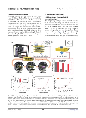
2.7. Device-level demonstration 3. Results and discussion
Schematic diagrams for the flexible printed circuit
board (fPCB) and the board layout were designed using 3.1. 3D printing of the polyanhydride
AUTODESK EAGLE (version 9.6.2). The components encapsulation layer
included a red LED (IN-S63ASR; Inolux, USA), 0402-in. Our 3D printing technique utilizes the DLP principle,
footprint capacitors, and six-turn double-layered coils for which involves dispersing the PBTPA solution and
wireless power transferring (resonant frequency: 13.56 applying UV irradiation to create an optimized unit layer
MHz). All components were mounted onto the fPCB with 50 μm thickness. We achieved the desired thickness
manufactured by an ISO-9001-compliant vendor, using of PBTPA by dividing it into thin unit layers, resulting in
solder paste (SMDLTLFP; Chip Quik, USA). The device superior waterproofing properties through both physical
measured 11 mm in width and 9 mm in length. The fPCB and chemical means (Figure 1). The layer-by-layer 3D
device, including the LED, was embedded in 1% agarose, printing process isolates polymer defects in each layer. The
containing PBS, and stored in a 37°C oven. decoupled defects in the unit layer increase the effective
Figure 1. 3D printing strategy of polyanhydride encapsulation for transient electronics. (A) Graphical scheme for 3D-printed polyanhydride encapsulation
to provide a longer penetration path through layer-by-layer printing. (B) The attenuation effect increases with the thickness of the screen-printed PBTPA,
evidenced by the decreased absorption coefficient (α) and transmittance (T) at 365 nm. (C) Increased lifetime of Mg resistor (300 nm of Mg pattern on 20
nm of Cr) when using 3D-printed PBTPA layer. (D) The lifetime exponentially increases with the thickness of the total encapsulation layer; lifetime was
evaluated as the time taken for the Mg resistor to reach a resistance of 200 Ω. (E) Measured lifetime increase (%) of the 3D-printed encapsulation layer
according to its number of stacking layer, relative to a screen-printed encapsulation layer. Abbreviations: PBTPA, polybutanedithiol 1,3,5-triallyl-1,3,5-
triazine-2,4,6(1H,3H,5H)-trione pentenoic anhydride; SP/500, screen-printed 500-μm-thick film; 3P/500, 3D-printed 500-μm-thick film.
Volume 10 Issue 5 (2024) 310 doi: 10.36922/ijb.3871