
Page 500 - IJB-10-3
P. 500
International Journal of Bioprinting 3D printing microgroove nerve conduits
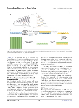
Figure 1. (a) Design specification of 3D-printed moulds with designs of 10/10/10 μm, 20/20/10 μm, 25/25/10 μm, and 30/30/10 μm; and (b) the procedures
for preparation of the microgrooved PCL or PCL/PLA substrates.
(Figure 1b). The solutions were left to evaporate in a area: 95 × 71 µm and 50× magnification). The roughness of
fume cabinet for 1 h, and the casted films were removed. the upper groove surface (400×) was assessed with a scan
Microgroove samples consisting of the designs, flat (no area of 10 × 7 µm (20, 25, and 30 µm microgrooves) and
microgrooves), 10/10/10 µm, 20/20/10 µm, 25/25/10 µm, 6 × 5 µm (10 µm microgroove). Images were post-processed
and 30/30/10 µm, are referred to as PCL-F, PCL-10, PCL- using Gwyddion software.
20, PCL-25, and PCL-30 or PCL/PLA-F, PCL/PLA-10,
PCL/PLA-20, PCL/PLA-25, and PCL/PLA-30, respectively. The casted microgroove thin films for SEM were
Different layer thicknesses (~10, 20, or 30 µm) of thin films sputter-coated (Q150R S, Quorum Technologies, UK) with
were produced by using different volumes of polymer gold/palladium (80/20) to obtain ~6 nm thick coating.
solution, and the thickness of casted films was inspected Images from the top surface of the microgroove thin film
with a digital calliper. Except for mechanical testing, 20 µm were captured and analysed using ImageJ software. 46
thick samples were utilised throughout the study. The surface roughness of the thin films was analysed
through AFM equipped with a ScanAsyst-Air probe
2.4. Morphology and roughness of moulds and
microgroove films (shape: pyramid; height: 10 µm; radius: <10 nm) in Peak
The 3D-printed moulds, PDMS moulds, and casted Force tapping mode. The topographic profiles refer to scan
microgroove films were assessed using an upright digital areas of 0.5 × 0.5 µm with a resolution of 512 × 512 pixels.
light microscope (VHX-5000, Keyence, Japan), a laser The image processing and roughness values measurement
scanning confocal microscope (LSCM; VK-X250, Keyence, were performed by Gwyddion software.
Osaka, Japan), a scanning electron microscope (SEM; 2.5. Thermal evaluation
Zeiss Sigma VP, Carl Zeiss, USA), and an atomic force Thermogravimetric analysis (TGA) of the PCL, PLA, and
microscope (AFM; Multimode 8-HR, Bruker, Germany). PCL/PLA samples (mass ~10 mg) was performed using TA
The LSCM with 120 nm lateral resolution using a 408 nm Instruments Q50 (TA Instruments, New Castle, USA). The
violet laser and a 16-bit photomultiplier to receive the laser test was carried out in an air atmosphere between 25 and
light was utilised to analyse the surface topography (scan 600°C with a heating rate of 10°C/min.
Volume 10 Issue 3 (2024) 492 doi: 10.36922/ijb.2725