
Page 66 - IJB-8-1
P. 66
AJ P of Bioelectrical Devices
®
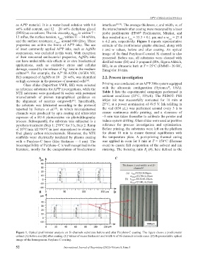
as AJ P material. It is a water-based solution with 0.8 interfaces [28,29] . The average thickness, t, and width, w, of
®
wt% solid content, and 12 – 20 wt% diethylene glycol the microchannels after coating were measured by a laser
(DEG) as co-solvent. The ink viscosity, η INK , is within 7 – probe profilometer (PF60 Profilometer, Mitaka), and
®
12 mPas, the surface tension, s INK , within 31 – 34 mN/m, they resulted in a t = 33.3 ± 0.1 μm and a w = 27.4
avg
avg
and the surface resistance, r INK , around 800 Ω/sq. These ± 4.2 μm, respectively. Figure 1 reports representative
properties are within the limits of AJ P inks. The use extracts of the profilometer graphs obtained, along with
®
of most commonly applied AJ P inks, such as AgNPs t and w values, before and after coating. An optical
®
suspensions, was excluded in this work. With exception image of the final Parylene-C-coated Si channel is also
of their renowned antibacterial properties, AgNPs inks presented. Before use, all substrates were cleaned with
can have undesirable side effects in in vitro bioelectrical distilled water (DI) and 2-propanol (IPA, Sigma Aldrich,
applications, such as oxidative stress and cellular BE), in an ultrasonic bath at T = 25°C (EMMI - 20 HC,
damage, caused by the release of Ag ions in the medium Emag) for 10 min.
+
culture . For example, the AJ SI-AJ20x (AGFA NV,
[25]
®
BE) composed of AgNPs at 10 – 20 wt%, was identified 2.2. Process investigation
as high cytotoxic in the presence of neuronal cells . ®
[26]
Glass slides (Superfrost VWR, BE) were selected Printing was conducted on an AJ P 300s system equipped
®
as reference substrates for AJ P investigations, while the with the ultrasonic configuration (Optomec , USA).
®
NTE substrates were pyrolized Si wafers with patterned Table 1 lists the experimental campaigns performed in
microchannels of proven topographical guidance on ambient conditions (22°C, 55%rh). The PEDOT: PSS
the alignment of neurites outgrowth . Specifically, inkjet ink was successfully sonicated for 10 min at
[27]
the substrate was fabricated according to the protocol 25°C, at a power atomization of 49.5 V. Ink refilling in
reported by Ferraro et al. , in which micropatterned the vial (850 μL) was performed around every 3 h to
[27]
channels were produced by spin coating and ultraviolet ensure continuous stable printing, and a clearance of
exposure of a SU-8 photoresistor via photolithography ~5 min was taken thereafter to calibrate the printer and
process. Subsequently, the substrate was subjected to a reduce system drifting. Glass slides were used as positive
pyrolysis treatment (Step 1: 270°C for 3 h, Step 2: Ramp reference for process investigation and optimization.
of 10°C/min till 950°C in inert atmosphere) to obtain the Before printing, the substrates were left on the platform
final glassy carbon microchannels. Moreover, the NTE for about 10 min to ensure thermal equilibrium with
scaffolds were electrically insulated by plasma coating the temperature plate. A post-printing thermal curing
with a Parylene-C layer (film thickness ~ 4 μm). The was applied in oven for 8 min at T = 150°C (Heraeus
biocompatibility of Parylene–C is well recognized in the oven) to ensure full evaporation of the solvent and ink
literature, mostly for the encapsulation of bioelectronic sintering. The focusing ratio R (#), here defined as the
f
A C
B D
Figure 1. Optical profilometer analysis on Si-channels substrates before and after Parylene-C coating. The figure shows a profilometer
extract (A) before and (B) after coating. (C) Values of mean thickness t and width w of Si-channels in both cases. (D) Representative optical
image of the homogenous Parylene-C coating.
52 International Journal of Bioprinting (2022)–Volume 8, Issue 1