
Page 71 - IJB-8-1
P. 71
Seiti, et al.
annealing time to validate the findings regardless the two couples of in series capacitors for the generation of
amount of material deposited (dose-dependent behavior) an alternated homogeneous spatial electric field across
and post-processing strategies. the microchannels patterned in the Si-based wafer. The
final aim is to stimulate orientation and cells morphology
2.5. Target application along the channels by applying a combined uniaxial and
Figure 3A schematically depicts the elements and bidirectional electrical-topographical cue. Figure 3B
functional principle of the intended device, which includes shows the entire fabrication procedure and Figure 3C
A B
C
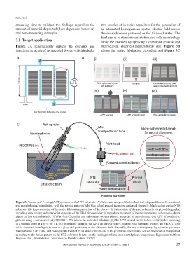
Figure 3. Aerosol Jet Printing (AJ P) process on the NTE substrate. (A) Schematic design of the bioelectrical integrated device for electrical
®
®
and morphological stimulation, with the printed pattern (light blue color) around the micro-patterned channels (black color) on the NTE
substrate. (B) Representation of the entire fabrication procedure of the device: (i) Fabrication of the microchannels via photolithography,
including spin coating and ultraviolet exposure of the SU-8 photoresistor; (ii) pyrolysis treatment of the micropatterned substrate to obtain
glassy carbon microchannels; (iii) Parylene-C coating and subsequent oxygen plasma treatment of the substrate; (iv) AJ P of conductive
®
patterns using a commercial inkjet PEDOT: PSS ink on the preheated substrate; (v) the AJ P printed circuit before and (iv) after annealing
®
in a thermal oven at 140°C for 1 h. (C) Schematic figure of the AJ P on the Parylene-C-coated NTE substrate. Firstly, the PEDOT: PSS
®
ink is atomized from liquid to mist in a glass vial positioned in the ultrasonic bath. Secondly, the mist is transported by a carrier gas into a
transportation PTFE tube, and consequently focused by an annular sheath gas in the print head. The focused aerosolized beam is then printed
according to the design pattern on the NTE substrate, located on the printing platform at a selected platen temperature. Figure adapted from
Degryse et al., International Conference on Biofabrication, 2021 .
[33]
International Journal of Bioprinting (2022)–Volume 8, Issue 1 57