
Page 16 - IJAMD-2-1
P. 16
International Journal of AI for
Materials and Design
Predicting thermal conductivity of sintered Ag
In this study, image processing and modeling simulation appropriate material properties to the current voxel block.
of microstructure images were performed using Since sintered nano-Ag is an isotropic material, distribution
MATLAB and Ansys, respectively. The results from the in the x-, y-, and z-directions are consistent. Therefore, 2D
batch calculation of the thermal conductivity of sintered models can be used to simulate the heat transfer behavior
nano-Ag microstructures enhanced the understanding of sintered nano-Ag, with microstructural characteristics.
of the physical relationship between sintered nano-Ag A plane model of nano-Ag and air was established, where
microstructure and heat transfer properties. the thermal conductivity of dense nano-Ag and air is 429
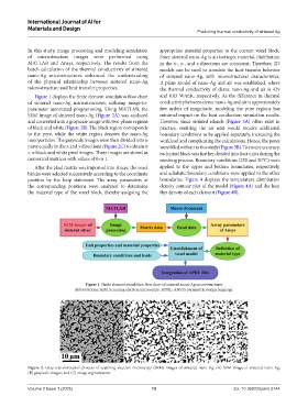
Figure 1 displays the finite element simulation flow chart and 0.03 W/mK, respectively. As the difference in thermal
of sintered nano-Ag microstructures, utilizing image-to- conductivity between dense nano-Ag and air is approximately
parameter automated programming. Using MATLAB, the five orders of magnitude, modeling the pore regions has
SEM image of sintered nano-Ag (Figure 2A) was analyzed minimal impact on the heat conduction simulation results.
and converted into a grayscale image with two-phase regions However, since isolated islands (Figure 3A) often exist in
of black and white (Figure 2B). The black region corresponds practice, omitting the air unit would require additional
to the pore, while the white region denotes the nano-Ag boundary conditions to be applied separately, increasing the
nanoparticles. The grayscale images were then divided into n workload and complicating the calculations. Hence, the pores
parts equally in the x and y directions (Figure 2C) to obtain n were filled with air in this study (Figure 3B). To ensure accuracy,
× n black and white pixel images. These images are stored as each pixel block was further divided into four units during the
numerical matrices with values of 0 or 1. meshing process. Boundary conditions (250 and 50℃) were
After the pixel matrix was imported into Ansys, the voxel applied to the upper and bottom boundaries, respectively,
blocks were selected successively according to the coordinate and adiabatic boundary conditions were applied to the other
position by the loop statement. The array parameters at boundaries. Figure 4 displays the temperature distribution
the corresponding positions were analyzed to determine density contour plot of the model (Figure 4A) and the heat
the material type of the voxel block, thereby assigning the flux density of each element (Figure 4B).
Figure 1. Finite element simulation flow chart of sintered nano-Ag microstructures
Abbreviations: SEM: Scanning electron microscopy; APDL: ANSYS parametric design language.
A B C
Figure 2. Gray transformation process of scanning electron microscopy (SEM) images of sintered nano-Ag: (A) SEM image of sintered nano-Ag;
(B) grayscale images; and (C) image segmentation.
Volume 2 Issue 1 (2025) 10 doi: 10.36922/ijamd.5744