
Page 57 - IJB-10-1
P. 57
International Journal of Bioprinting Microfluidic-assisted 3D bioprinting
2. Approaches for biomicrofluidic (generally glass or PDMS) through air or oxygen plasma
18
devices fabrication treatment (Figure 2a).
Microfluidic devices are composed of microchannels Although traditional microfluidic manufacturing may
with cross-sectional dimensions typically ranging achieve elevated resolution (down to the order of 10 nm),
from 0.1 to 1000 μm. The flow regime induced by sub- the process presents several drawbacks. Photolithography,
19
millimetric confinement is called laminar and implies indeed, is an expensive and time-consuming process and is
the predominance of ordered flow patterns, which are not accessible to most chemists, biochemists, and biologists.
only subjected to diffusive mixing at the fluids interface A significant obstacle to adopting photolithography for the
rather than stochastic mixing arising from convective quick manufacture of microfluidic devices is the laborious
20
forces. 13,14 In the laminar domain, indeed, flow profiles are procedure needed to obtain the photomask along with
deterministic and thus can be mathematically modeled the inability to realize non-planar structures.
and digitally simulated, allowing to obtain unparalleled 2.2. Modern approaches in microfabrication
level of control over the spatiotemporal dynamics of fluids 21
and molecules. 15,16 Leveraging modern approaches such as additive or
subtractive manufacturing to fabricate molds for PDMS
22
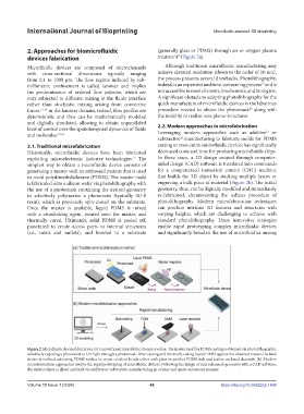
2.1. Traditional microfabrication casting or even entire microfluidic devices has significantly
Historically, microfluidic devices have been fabricated decreased costs and time for producing microfluidic chips.
exploiting microelectronic industry technologies. The In these cases, a 3D design created through computer-
17
simplest way to obtain a microfluidic device consists of aided design (CAD) software is translated into commands
generating a master with an embossed pattern that is used for a computerized numerical control (CNC) machine
to mold polydimethylsiloxane (PDMS). The master mold that builds the 3D object by stacking multiple layers or
is fabricated onto a silicon wafer via photolithography with engraving a bulk piece of material (Figure 2b). The initial
the use of a photomask containing the desired geometry geometry, thus, can be digitally modified and immediately
to selectively polymerize a photoresist (typically SU-8 re-fabricated, circumventing the tedious procedure of
resin), which is previously spin-coated on the substrate. photolithography. Modern microfabrication techniques
Once the master is available, liquid PDMS is mixed can produce intricate 3D features and structures with
with a crosslinking agent, poured onto the master, and varying heights, which are challenging to achieve with
thermally cured. Ultimately, solid PDMS is peeled off, standard photolithography. These innovative strategies
punctured to create access ports to internal structures enable rapid prototyping complex microfluidic devices
(i.e., inlets and outlets), and bonded to a substrate and significantly broaden the use of microfluidics among
Figure 2. Microfluidic device fabrication. (a) Conventional microfabrication procedure. The master mold for PDMS casting is obtained via photolithography,
selectively exposing a photoresist to UV light through a photomask. After casting and thermally curing liquid PDMS against the obtained master, the final
device is realized activating PDMS surface to create covalent bonds either with glass or another PDMS slab and realize enclosed channels. (b) Modern
microfabrication approaches involve the rapid prototyping of microfluidic devices. Following the design of microchannels geometry with a CAD software,
the virtual object is sliced and built via additive or subtractive manufacturing in a faster and more convenient manner.
Volume 10 Issue 1 (2024) 49 https://doi.org/10.36922/ijb.1404