
Page 96 - MSAM-3-3
P. 96
Materials Science in Additive Manufacturing Wide-angle broadband MMA with CB-CIP/PLA
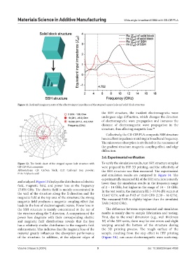
Figure 11. Real and imaginary parts of the effective input impedance of the stepped square hole and solid block structure
the SSH structure, the incident electromagnetic wave
undergoes edge diffraction, which changes the direction
of electromagnetic wave propagation and increases the
distance of electromagnetic wave propagation in the
structure, thus affecting magnetic loss. 44
Collectively, the CB-CIP/PLA composite SSH structure
has excellent impedance matching in broadband frequency.
The microwave absorption is attributed to the resonance of
the gradient structure, magnetic coupling effect, and edge
diffraction.
3.6. Experimental verification
Figure 12. The Smith chart of the stepped square hole structure with To verify the simulation results, test SSH structure samples
CB-CIP/PLA composite were prepared by FFF 3D printing, and the reflectivity of
Abbreviations: CB: Carbon black; CIP: Carbonyl iron powder; the SSH structure was then measured. The experimental
PLA: Polylactic acid
and simulation results are compared in Figure 14. The
experimentally measured RL of the SSH structure is mostly
and analyzed. Figure 13 displays the distribution of electric lower than the simulation results in the frequency range
field, magnetic field, and power loss at the frequency of 2 – 14 GHz, but higher in the range of 14 – 18 GHz.
15.056 GHz. The electric field is mainly concentrated in In the test results, the minimum RL (−35.94 dB) occurs at
the wall of the structure along the X-direction and the 13.647 GHz, with an EAB of 15.61 GHz (2.39 – 18 GHz).
magnetic field at the top area of the structure; the strong The measured EAB is slightly higher than the simulated
magnetic field produces a magnetic coupling effect that EAB (14.032 GHz).
leads to the loss of electromagnetic waves. Power loss in
the SSH structure is mainly concentrated at the top of The difference between experimental and simulation
the structure along the Y-direction. A comparison of the results is mainly due to sample fabrication and testing.
power loss diagrams with their corresponding electric First, due to the small dimension (e.g., wall thickness
and magnetic field distributions reveals that the loss W) of the SSH units, there may be size errors and slight
has a relatively similar distribution to the magnetic field warping around the bottom of the structure during
enhancement. This indicates that the magnetic loss of the the 3D printing process. The rough surface of the
material greatly influences the absorption performance sample, resulting from the step effect in FFF printing
of the structure. In addition, at the adjacent edges of (Figure 3A), can cause electromagnetic wave scattering.
Volume 3 Issue 3 (2024) 9 doi: 10.36922/msam.4158