
Page 14 - MSAM-3-4
P. 14
Materials Science in Additive Manufacturing Additive manufacturing of active optics
A
C
B
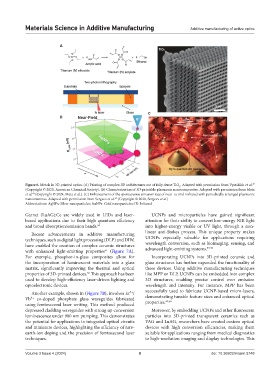
Figure 6. Metals in 3D‑printed optics. (A) Printing of complex 3D architectures out of fully dense TiO . Adapted with permission from Vyatskikh et al.
37
2
(Copyright © 2020, American Chemical Society). (B) Characterization of 3D-printable plasmonic nanocomposites. Adapted with permission from Mata
et al. (Copyright © 2024, Mata et al.). (C) Enhancement of the spontaneous emission rate of near- to mid-infrared with periodically arranged plasmonic
49
nanoantennas. Adapted with permission from Sergeev et al. (Copyright © 2020, Sergeev et al.)
38
Abbreviations: AgNPs: Silver nanoparticles; AuNPs: Gold nanoparticles; IR: Infrared
Garnet (LuAG):Ce are widely used in LEDs and laser- UCNPs and microparticles have gained significant
based applications due to their high quantum efficiency attention for their ability to convert low‑energy NIR light
and broad absorption/emission bands. 50 into higher-energy visible or UV light, through a non-
Recent advancements in additive manufacturing linear anti-Stokes process. This unique property makes
techniques, such as digital light processing (DLP) and DIW, UCNPs especially valuable for applications requiring
have enabled the creation of complex ceramic structures wavelength conversion, such as bioimaging, sensing, and
39,42
with enhanced light-emitting properties (Figure 7A). advanced light-emitting systems.
51
For example, phosphor-in-glass composites allow for Incorporating UCNPs into 3D‑printed ceramic and
the incorporation of luminescent materials into a glass glass structures has further expanded the functionality of
matrix, significantly improving the thermal and optical these devices. Using additive manufacturing techniques
properties of 3D-printed devices. This approach has been like MPP or DLP, UCNPs can be embedded into complex
52
used to develop high-efficiency laser-driven lighting and 3D structures, enabling precise control over emission
optoelectronic devices. wavelength and intensity. For instance, MPP has been
successfully used to fabricate UCNP‑based micro‑lasers,
+
Another example, shown in (Figure 7B), involves Er³ /
Yb³ co-doped phosphate glass waveguides fabricated demonstrating tunable feature sizes and enhanced optical
+
43,54
using femtosecond laser writing. This method produced properties.
depressed cladding waveguides with strong up-conversion Moreover, by embedding UCNPs and other fluorescent
luminescence under 980 nm pumping. This demonstrates particles into 3D-printed transparent ceramics such as
the potential for applications in integrated optical circuits YAG and LuAG, researchers have created custom optical
and miniature devices, highlighting the efficiency of rare- devices with high conversion efficiencies, making them
earth-ion doping and the precision of femtosecond laser suitable for applications ranging from medical diagnostics
techniques. to high-resolution imaging and display technologies. This
Volume 3 Issue 4 (2024) 8 doi: 10.36922/msam.5748