
Page 17 - MSAM-3-4
P. 17
Materials Science in Additive Manufacturing Additive manufacturing of active optics
A C
B
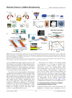
Figure 9. Printing of nanocomposites for multifunctional 3D optics. (A) Multimaterial filament inks used for printing of optical structures. Adapted with
61
permission from Loke et al. (Copyright © 2019, Loke et al.). (B) Printing of inflight fiber for 3D optoelectronic and sensing architectures. Adapted with
62
permission from Wang et al. (Copyright © 2020, Wang et al.). (C) 2PP of nanocomposites for fused silica glass structures. Adapted with permission from
63
Kotz et al. (Copyright © 2021, Kotz et al.)
Abbreviations: 2PP: Two‑photon polymerization; EDX: Energy‑dispersive X‑ray; PEDOT: PSS: Poly(3,4‑ethylenedioxythiophene) polystyrene sulfonate;
PEO: Polyethylene oxide; TEM: Transmission electron microscopy; XPS: X‑ray photoelectron spectroscopy
terms of scalability and design complexity. However, with Furthermore, the versatility of 3D printing enables
3D printing, it is now possible to design and manufacture the incorporation of a wide range of materials, from
highly customized optoelectronic devices with intricate semiconductors to organic polymers, within a single
71
geometries and precise material placements, resulting in optoelectronic device. This multifunctionality allows
enhanced performance, greater flexibility, and the ability for the development of devices that can both detect and
to incorporate multifunctional capabilities. 70 emit light, leading to new possibilities in fields such as
One of the key advancements enabled by 3D printing in optical communications, environmental monitoring, and
optoelectronics is the integration of QDs and organic light- biomedical devices. The ability to create these complex,
emitting materials into optoelectronic structures. QDs multi-material structures through additive manufacturing
offer tunable emission wavelengths that can be adjusted represents a major shift in the production and design
based on their size, making them ideal for displays, sensors, of optoelectronic devices, offering unprecedented
and wearable devices. Additive manufacturing allows opportunities for innovation in the field. Figure 11 shows
for the precise deposition of QDs within optoelectronic printing of optoelectronic device for various applications. 72-75
components, enhancing the efficiency and functionality
of these devices. This has broad implications for next- 4.3. Integrated photonics: Advances in additive
generation technologies, including ultra-thin, flexible manufacturing for photonic circuits
displays and wearable electronics that require high- Integrated photonics refers to the miniaturization and
resolution, energy-efficient light emission. 4 integration of multiple optical components, such as
Volume 3 Issue 4 (2024) 11 doi: 10.36922/msam.5748