
Page 15 - MSAM-3-4
P. 15
Materials Science in Additive Manufacturing Additive manufacturing of active optics
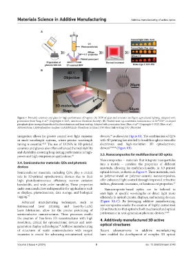
A
B
Figure 7. Printable ceramics and glass for high-performance 3D optics. (A) DIW of glass and ceramics intelligent agricultural lighting. Adapted with
permission from Yang et al. (Copyright © 2023, American Chemical Society). (B) Guided-wave up-conversion luminescence in Er /Yb co-doped
51
3+
3+
phosphate glass waveguide produced by direct femtosecond laser writing. Adapted with permission from Zhou et al. (Copyright © 2022, Zhou et al.)
53
Abbreviations: CASN‑phosphor‑in‑glass: CaAlSiN3:Eu2+ Phosphors in Glass; DIW: Direct ink writing; UV: Ultraviolet
integration allows for greater control over light emission devices, as shown in Figure 8A. The combination of QDs
59
in multi-wavelength systems, where precise wavelength with 3D printing has also led to breakthroughs in wearable
tuning is essential. 42,55 The use of UCNPs in 3D‑printed electronics and high-resolution 3D optoelectronic
ceramics and glasses also offers enhanced thermal stability devices 57,58,60 (Figure 8B).
and durability, ensuring long-lasting performance in high-
power and high-temperature applications. 56 3.5. Nanocomposites for multifunctional 3D optics
Nanocomposites – materials that integrate nanoparticles
3.4. Semiconductor materials: QDs and photonic into a matrix – combine the properties of different
devices materials, allowing for multifunctionality in 3D-printed
Semiconductor materials, including QDs, play a critical optical devices, as shown in Figure 9. These materials, such
role in 3D-printed optoelectronic devices due to their as polymer-metal or polymer-ceramic nanocomposites,
high photoluminescence efficiency, narrow emission offer enhanced light control through improved refractive
bandwidth, and wide color tunability. These properties indices, plasmonic resonance, or luminescent properties. 37
make semiconductors indispensable for applications such Nanocomposite-based optics can be tailored to
as displays, photodetectors, data storage, and biological emit light at specific wavelengths or direct light more
tagging. 57 efficiently in optical circuits, displays, and sensing devices.
Advanced manufacturing techniques, such as (Figure 9A-C). By leveraging additive manufacturing,
femtosecond laser printing and layer-by-LuAG nanocomposites enable the creation of highly customized
layer fabrication, allow for the precise patterning of 3D architectures that optimize both mechanical and optical
semiconductor nanostructures. These processes enable performance in next-generation photonic devices. 61-65
the creation of free-form 3D nanostructures with high 4. Additively manufactured 3D active
resolution, critical for optoelectronic devices and next-
generation display technologies. Additive manufacturing optical structures
58
of structures of oxide semiconductors with oxygen Recent advancements in additive manufacturing
vacancies is crucial for advancing miniaturized optical have enabled the development of complex 3D optical
Volume 3 Issue 4 (2024) 9 doi: 10.36922/msam.5748