
Page 18 - MSAM-3-4
P. 18
Materials Science in Additive Manufacturing Additive manufacturing of active optics
A B
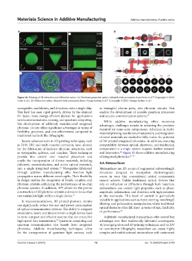
Figure 10. Printing of 3D refractive and diffractive optics. (A) Freeform geometric optics. Adapted with permission from Ocier et al. (Copyright © 2020,
68
Ocier et al.). (B) Diffractive optics. Adapted with permission from Orange Kedem et al. (Copyright © 2023, Orange Kedem et al.)
69
waveguides, modulators, and detectors, onto a single chip. as entangled photon pairs, into photonic circuits. This
This field has seen rapid growth, driven by the demand enables the development of scalable quantum processors
for faster, more energy-efficient devices for applications and secures communication systems. 79
in telecommunications, sensing, and quantum computing. While additive manufacturing offers numerous
The development of additively manufactured integrated advantages, challenges remain in achieving the precision
photonic circuits offers significant advantages in terms of required for nano-scale components. Advances in multi-
flexibility, precision, and cost-effectiveness compared to material printing, resolution enhancement, and integration
traditional methods like lithography. of novel materials are needed to fully realize the potential
Recent advancements in 3D printing techniques, such of 3D-printed integrated photonics. In addition, ensuring
as DIW, 2PP, and multi‑material extrusion, have allowed compatibility between optical, electronic, and mechanical
for the fabrication of intricate photonic structures, such components in a single system requires further research
as waveguides, splitters, and couplers. These techniques and innovation. Figure 12 shows additive manufacturing
80
provide fine control over material placement and of integrated photonics. 81-84
enable the incorporation of diverse materials, including
polymers, semiconductors, and active optical materials, 4.4. Metasurfaces
into a single integrated system. Waveguides fabricated Metasurfaces are 2D arrays of engineered subwavelength
76
through additive manufacturing offer low-loss light structures designed to manipulate electromagnetic
propagation across different wavelengths. Their flexibility waves in ways that conventional optical components
in design enables the integration of bends, couplers, and cannot achieve. Unlike traditional optical devices that
photonic crystals, enhancing the performance of on-chip rely on refraction or diffraction through bulk materials,
photonic systems. In addition, 2PP allows for the precise metasurfaces can control light properties such as phase,
construction of 3D photonic crystals and micro-lenses that amplitude, polarization, and direction with high precision
can manipulate light within a single device. 77 at the nanoscale. This level of control is particularly
In telecommunications, 3D-printed photonic circuits valuable in applications such as beam steering, wavelength
can significantly reduce the size and power consumption filtering, and polarization manipulation, where traditional
of optical communication systems. The ability to integrate optical elements often fall short in terms of size, flexibility,
80
modulators, lasers, and detectors into a single device leads or performance.
to more compact and efficient systems that are crucial for Additively manufactured metasurfaces offer several key
high-speed data transmission. Quantum computing and advantages over their traditionally fabricated counterparts.
78
quantum communication also benefit from integrated By leveraging advanced 3D printing techniques, such as 2PP
photonics. Additive manufacturing techniques allow or nanoimprint lithography, researchers can create highly
for the incorporation of quantum light sources, such complex and multifunctional metasurfaces with customized
Volume 3 Issue 4 (2024) 12 doi: 10.36922/msam.5748