
Page 19 - MSAM-3-4
P. 19
Materials Science in Additive Manufacturing Additive manufacturing of active optics
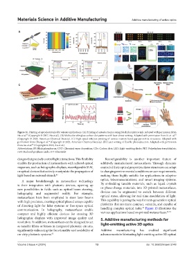
A B
C D
Figure 11. Printing of optoelectronics for various applications. (A) Printing of optoelectronics using black phosphorus ink. Adapted with permission from
72
Hu et al. (Copyright © 2017, Hu et al.). (B) Multicolor afterglow carbon dot patterns with laser direct writing. Adapted with permission from Li et al.
73
(Copyright © 2024, American Chemical Society). (C) High‑speed solution printing of various narrow‑band‑gap perovskite structures. Adapted with
74
permission from Chang et al. (Copyright © 2023, American Chemical Society). (D) Laser writing of flexible photodetectors. Adapted with permission
75
from An et al. (Copyright © 2018, An et al.)
Abbreviations: BP: Black phosphorus; CVD: Chemical vapor deposition; CDs: Carbon dots; LED: Light‑emitting diode; PET: Polyethylene terephthalate;
rGO: Reduced graphene oxide; UV: Ultraviolet
designs that precisely control light interactions. This flexibility Reconfigurability is another important feature of
enables the production of metasurfaces with tailored optical additively manufactured metasurfaces. Through dynamic
responses, such as holographic displays, reconfigurable SLM, control of their optical properties, these structures can adapt
or optical devices that actively manipulate the propagation of to changing environmental conditions or user requirements,
light based on external stimuli. 85 making them highly suitable for applications in adaptive
A major breakthrough in metasurface technology optics, telecommunications, and smart imaging systems.
is their integration with photonic devices, opening up By embedding tunable materials, such as liquid crystals
new possibilities in fields such as optical beam steering, or phase-change materials, into 3D-printed metasurfaces,
holography, and augmented reality. For example, devices can be engineered to switch between different
metasurfaces have been employed to steer laser beams optical states, allowing for real-time modulation of light.
with high precision, creating optical phased arrays capable This capability is paving the way for next-generation optical
of directing light for lidar systems or free-space optical platforms that are more compact, versatile, and capable of
78
communication. In holography, metasurfaces enable handling complex optical tasks. Figure 13 illustrates the
compact and highly efficient devices for creating 3D various applications based on printed metasurfaces. 86-91
holographic displays with improved image quality and 5. Additive manufacturing methods for
resolution. In addition, metasurfaces can be designed to act
as tunable filters or lenses in integrated photonic circuits, light-emitting active 3D optics
significantly enhancing the functionality and scalability of Additive manufacturing has enabled significant
on-chip photonic systems. 85 advancements in fabricating light-emitting active 3D optical
Volume 3 Issue 4 (2024) 13 doi: 10.36922/msam.5748