
Page 24 - MSAM-3-4
P. 24
Materials Science in Additive Manufacturing Additive manufacturing of active optics
A
B
C
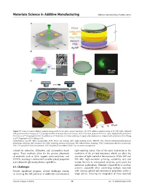
Figure 15. Cases of various additive manufacturing methods for active optical structures. (A) DIW additive manufacturing of 3D QD-LEDs. Adapted
114
with permission from Kong et al. (Copyright © 2014, American Chemical Society). (B) SLS for short‑pulse UCNP micro‑laser. Adapted with permission
108
from Jiao et al. (Copyright © 2021, Royal Society of Chemistry). (C) Inkjet printing of organic printed photonics. Adapted with permission from Zhang
et al. (Copyright © 2015, Zhang et al.)
40
Abbreviations: Ag NP: Silver nanoparticle; DIW: Direct ink writing; LED: Light‑emitting diode; PEDOT: PSS: Poly(3,4‑ethylenedioxythiophene)
polystyrene sulfonate; QD: Quantum dot; SEM: Scanning electron microscopy; SLS: Selective laser sintering; TEM: Transmission electron microscopy;
Poly‑TPD: poly[N,N'‑bis(4‑butylphenyl)‑N,N'‑bis(phenyl)‑benzidine; UCNP: Up‑conversion nanoparticle
critical for refractive, diffractive, and metasurface-based light‑emitting optics. One of the main limitations is the
optics. These methods allow for the precise placement resolution of the printed structures, which can affect the
of materials such as QDs, organic semiconductors, and precision of light control at the nanoscale. While 2PP and
UCNPs, resulting in devices with tunable optical properties SLS offer high-resolution printing, scalability, and cost
and enhanced light manipulation capabilities. remain barriers to widespread adoption, particularly for
industrial applications. Material compatibility is another
6.1. Challenges concern, especially when combining multiple materials
Despite significant progress, several challenges remain with varying optical and mechanical properties within a
in realizing the full potential of additively manufactured single device. Ensuring the integration of these materials
Volume 3 Issue 4 (2024) 18 doi: 10.36922/msam.5748