
Page 25 - MSAM-3-4
P. 25
Materials Science in Additive Manufacturing Additive manufacturing of active optics
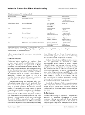
Table 2. Comparison of 3D printing methods
Printing method Materials Advantages Disadvantages
FDM Thermoplastic polymers • Simple • Low resolution
• Cheap • Roughness issue
• Limitation in complexity
Polyjet (material jetting) Photocurable polymer • Multi‑material • High cost
• Smooth surface
• High quality
DIW Polymers, ceramics • Diverse material • Low resolution
• Versatility • Fragile
• Post‑curing
SLA/DLP Photocurable resin • Smooth surface • Single material
• Recyclable raw material • Limited material
• Resin absorbs moisture
DLW Photoresist, photocurable polymer • High resolution • High cost
• No need for support • Limited material
• Time‑consuming
SLS Metal powder, ceramic powder, polymer powder • No need for support • Roughness issue
• Recyclable raw material • High cost
• High quality • Post‑processing
Adapted with permission from Jeong et al. (Copyright © 2020, Jeong et al.).
111
Abbreviations: DIW: Direct ink writing; DLP: Digital light processing; DLW: Direct laser writing; FDM: Fused deposition modeling; SLA:
Stereolithography; SLS: Selective laser sintering.
without compromising their performance is an ongoing these challenges will pave the way for scalable quantum
challenge. communication systems and processors, revolutionizing
secure communications and quantum computing.
6.2. Future prospects
Similarly, AR applications highlight both the promise
The future of additive manufacturing in optics will likely and the opportunities for innovation in additive
see improvements in multi-material printing, resolution, manufacturing. While achieving a balance between
and speed, allowing for the production of highly lightweight designs and structural robustness remains a
customized, functional optical components at lower costs. complex task, new developments in composite materials
Innovations in materials science, such as the development and multi-material printing continue to bridge this gap.
of new photopolymers, organic-inorganic hybrids, and Advances in metasurface technology are also enabling
responsive materials, will further expand the capabilities the creation of high-resolution, wide field-of-view optics
of 3D-printed optics. In addition, advancements in that meet the demanding requirements of AR systems.
116
metasurface technology will enable the creation of These efforts are expected to yield compact, efficient,
reconfigurable optical systems with dynamic control over and cost‑effective AR devices, transforming wearable
light propagation, polarization, and wavelength. technology and enhancing user experiences in areas such
Emerging fields such as QDs, augmented reality (AR), as entertainment, education, and healthcare. 117
and medical imaging will also benefit significantly from Overall, the combination of additive manufacturing and
these advancements, despite the challenges they are currently advanced photonic materials holds tremendous promise
facing. In quantum photonics, the nanoscale precision for the future of optical device fabrication, leading to
required for quantum light sources and waveguides presents breakthroughs in telecommunications, sensing, imaging,
an ambitious target for additive manufacturing technologies. and more.
However, the continuous evolution of high‑resolution
techniques such as 2PP and the integration of cutting‑ 7. Conclusion
edge quantum materials hold the potential to meet these Additive manufacturing has emerged as a transformative
demands. As encapsulation methods advance, addressing approach for fabricating light-emitting 3D optical
115
the sensitivity of QDs to external factors such as heat, light, structures, offering unprecedented design freedom,
and environmental fluctuations will enhance the stability material versatility, and precision in the creation of
and reliability of quantum devices. Successfully overcoming complex optical components. Through methods such as
Volume 3 Issue 4 (2024) 19 doi: 10.36922/msam.5748