
Page 17 - MSAM-3-2
P. 17
Materials Science in Additive Manufacturing Functional materials for AM
3D printing technology has emerged as an alternative technologies underscore the versatility and efficiency of
that overcomes the limitations of conventional fabrication perovskites in converting light into electrical energy for
methods. It enables the fabrication of complex structures, various practical applications.
optimization of material usage, and cost-effective Inkjet printing achieves a high PCE of more than 21%,
production. In particular, it has been employed for replacing the conventional spin coating method due to
fabricating perovskite layers using inkjet printing, difficulties in scaling up to large areas. This advancement
90
meniscus printing, 91 electrohydrodynamic (EHD) was facilitated by utilizing a high-concentration precursor
printing, FDM, and DIW. However, securing high- to effectively form absorption layers thicker than 1 μm,
93
92
94
quality and stable inks remains a significant challenge. and by streamlining the manufacturing process through
Technological advancements in the fabrication and a single-ink approach. Perovskite photodetectors with
95
performance of perovskite materials using 3D printing high resolution, flexibility, and wide color range have been
technology are detailed in Table 4, highlighting their fabricated using EHD printing, overcoming the limitations
application in devices such as solar cells, sensors, and of fabricating multi-spectral semiconductors. This printing
LEDs. technique successfully produced high-quality perovskite
3.3.1. Photovoltaic effect dot arrays with 1 μm precision, presenting the potential
for future wide-color photodetector and artificial vision
Perovskite solar cells (PSCs) and photodetectors both systems. 96
leverage the light absorption properties of perovskites
to generate electrical signals from light energy. In PSCs, 3.3.2. Perovskite displays
light induces the generation of electron-hole pairs within In perovskite LEDs and through photoluminescence in
the active perovskite layer, which are, then, transported perovskites, the interplay of electrons and holes is crucial
through the hole transport layer (HTL) and electron for the conversion of electrical and absorbed light energy
transport layer (ETL) to electrodes, thereby transforming into emitted light of various wavelengths. Electron-hole
light into electricity. Similarly, perovskite photodetectors recombination within the perovskite layer is key to the
generate electron-hole pairs on exposure to light, guiding efficiency of light emission in LEDs, where the introduction
them toward electrodes to produce electrical signals for of various nanoparticles allows for a spectrum of colors
detecting light intensity and wavelength. These applications with high purity. Photoluminescence, on the other hand,
are pivotal in various fields, such as environmental involves the absorption of photons that excite electrons to
monitoring, image sensing, and optical communication, higher energy states. Following this excitation, some energy
requiring high sensitivity and rapid response times. These is lost, and the remaining energy is emitted as light when the
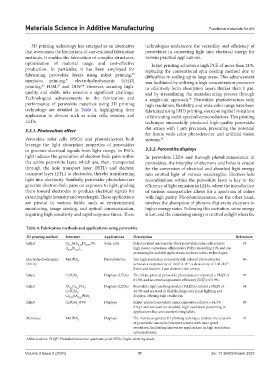
Table 4. Fabrication methods and applications using perovskite
3D printing method Structure Applications Description References
Inkjet Cs MA FA , Pb Solar cells Inkjet-printed micrometer-thick perovskite solar cells achieve 95
0.75
0.15
0.1
(I Br ) high power conversion efficiencies (PCEs) exceeding 21% and are
0.85
0.15 3
promising for scalable applications in photovoltaic technologies.
Electrohydrodynamic MAPbX 3 Photodetector The high-resolution perovskite full-colored photodetector 96
-1
(EHD) achieves a responsivity of 14.97 A W , a detectivity of 1.41×10
12
Jones and features 1 μm diameter dot arrays.
Inkjet CsPbBr Displays (LEDs) The inkjet-printed perovskite photodetector reported a PLQY of 97
3
61.8% and an external quantum efficiency (EQE) of 5.9%.
Inkjet FA Cs PbI , Displays (LEDs) Perovskite light-emitting diodes (PeLEDs) exhibit a PLQY of 98
3
0.2
0.8
CsPbBr , 14.3% and are used in flexible, large-area panel lighting and
3
Cs EA PbBr displays, offering high resolution.
0.75 0.25 3
Inkjet CsPbBr -PVP Displays Inkjet-printed perovskite nanocomposites achieve a 64.3% 99
3
PLQY and are used for detailed, high-resolution patterning in
applications like anticounterfeiting labels.
Meniscus MAPbX 3 Displays The meniscus-guided 3D printing technique enables the creation 91
of perovskite nanowire heterostructures with nano-pixel
resolution, facilitating innovative applications in high-resolution
optoelectronics.
Abbreviations: PLQY: Photoluminescence quantum yield; LEDs: Light-emitting diode.
Volume 3 Issue 2 (2024) 11 doi: 10.36922/msam.3323