
Page 17 - manuscript_ijb05583
P. 17
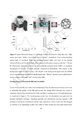
Figure 5: Optical Detection Setup A) CAD of the fluorescent detection setup. Blue dot = light

               source, green dot = holder + microfluidic device, red dot = photodiode. Cross-section detailing

               optical  path  of  excitation  (blue)  and  emission  (green)  light,  and  view  of  the  passing
               microscaffold as seen by photodiode (when replaced with camera system), scale bar = 100 µm

               B)  Fluorescent  emission  spectrum  of  microscaffolds  produced  from  ZrHyb  at  excitation

               wavelength  of  360  nm.  C)  Light  intensity  measured  by  photodiode:  “BG  empty”  is  the
               background signal of optical device, “BG sheath” is the background signal when the PDMS

               device was added and flushed with sheath liquid only, “Halves” denotes microscaffold-halves
               used to emulate debris and “Full” denotes intact BBs.


               Sorting process of buckyball (BB) microscaffolds


               To sort microscaffolds, two values were manipulated. First, the fluorescent intensity of an event

               to  determine  the  quality  of  the  BB  and  second,  the  timing  offset  between  two  events  to

               determine whether they would interfere with each other’s sorting process. The underlying logic
               is visualized in Figure 6. The incoming data stream from the photodiode was supervised for

               intensity  threshold  crossings.  Threshold  upwards  and  downwards  crossing  signaled  a  BB

               entering or leaving the detection area on the chip, respectively. These events were then flagged
               as sortable or not depending on their time offset to other events and their peak fluorescence


                                                           16