
Page 152 - MSAM-4-3
P. 152
Materials Science in Additive Manufacturing L-PBF Ti-10Ta-2Nb-2Zr: Microstructure and Strength
high-density components were successfully manufactured Society for Testing and Materials (ASTM) E8/E8M
within similar parameter ranges (Table 1). The processing standard with a gauge length of 15 mm and a diameter of
parameters were systematically varied to investigate their 3 mm.
influence on densification behavior and microstructural
evolution. The volumetric energy density (E) was calculated 2.3. Heat treatments
using Equation I. The selected specimens were heat-treated using the
following parameters: vacuum annealing at 900°C for 1 h,
P
E (I) followed by furnace cooling. The samples were heated at
Vh t a rate of 10°C/min to the target temperature in a vacuum
where P is laser power (W); V is scanning speed (mm/s); furnace (Carbolite Gero, UK) at a vacuum level of
−5
h is hatch spacing (μm); and t is layer thickness (μm). 10 mbar.
Cubic samples (10 × 10 × 10 mm ) were fabricated The selection of heat treatment temperature was based
3
for density measurements and microstructural on differential scanning calorimetry (DSC) analysis, which
characterization. For mechanical testing, cylindrical tensile identified the β-transus temperature range for the Ti-10Ta-
specimens were produced according to the American 2Nb-2Zr alloy. The annealing temperature of 900°C was
A B
D
C
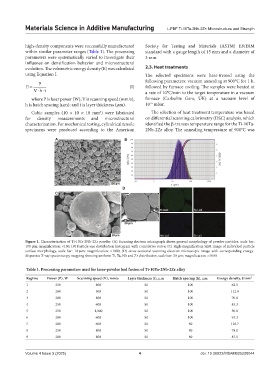
Figure 1. Characterization of Ti-10Ta-2Nb-2Zr powder. (A) Scanning electron micrograph shows general morphology of powder particles, scale bar:
100 μm; magnification: ×150; (B) Particle size distribution histogram with cumulative curve; (C) High-magnification SEM image of individual particle
surface morphology, scale bar: 10 μm; magnification: ×1000; (D) cross-sectional scanning electron microscopic image with corresponding energy-
dispersive X-ray spectroscopy mapping showing uniform Ti, Ta, Nb and Zr distribution, scale bar: 30 μm; magnification: ×1000
Table 1. Processing parameters used for laser‑powder bed fusion of Ti‑10Ta‑2Nb‑2Zr alloy
Regime Power (P), W Scanning speed (V), mm/s Layer thickness (t), μm Hatch spacing (h), μm Energy density, J/mm 3
1 250 800 50 100 62.5
2 280 500 50 100 112.0
3 280 800 50 100 70.0
4 250 600 50 100 83.3
5 250 1,000 50 100 50.0
6 280 600 50 100 93.3
7 280 600 50 80 116.7
8 250 800 50 80 78.1
9 280 800 50 80 87.5
Volume 4 Issue 3 (2025) 4 doi: 10.36922/MSAM025220044