
Page 75 - DP-1-1
P. 75
Design+ Defect-oriented BIST for AMS circuits
Table 3. Mapping the detection of each defect by monitoring the respective node
Fault M1 M2 M3 M4 M5 M6 M7 M8 M9 M10
Drain-open V out V out V G1 V out V G8 V G1 V G1 V out V G8 V G8
(1 µV) (1.73V) (761 mV) (588 mV)
Source-open V out V out V G1 V out V G8 V G1 V G1 V out V G8 V G8
(1.31 V) (1.73V) (690 mV) (642 mV)
Gate-open V out V out V G1 V out V G8 V G1 V G1 V out V G8 V G8
(65 mV) (1.73V) (588 mV) (588 mV)
Gate-drain short V G1 V out V out V G8 V G8 V out V G1 V out V G8 V G8
(1.94 V) (1.62 V) (1.48 V) (1.48 V)
Gate-source short V out V out V out V G8 V G8 V out V out V out V G8 V out
(1.94 V) (1.47 V) (1.76 V) (1.47 V) (1.94 V) (666 mV) (907 mV)
Drain-source short V V V V V V V V V V
G1 out out G8 G8 G8 out G1 G1 out
(148 mV) (1.76 V) (1.91 V) (8 mV)
Note: Each color represents each node.
Abbreviations: V V : Gate voltage; V : Output voltage.
G1, G8 out
defect coverage, V G1_INV and V G8_INV should have switching
threshold voltages of 2.1 V and 1.25 V respectively.
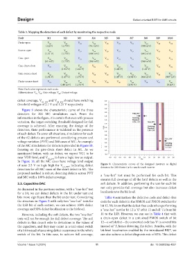
Figure 9 shows the characteristic curve of the three
detectors for 200 MC simulations each. From the
information in the figure, it is certain that even with process
variation, the target switching threshold designed for full
coverage is achieved. After ensuring the design of the
detectors, their performance is validated in the presence
of each defect. To cover all situations, simulations for each
of the 62 defects are performed considering process and
voltage variation (PVT) and 200 cases of MC. An example
of the MC simulations for defects is provided in Figure 10,
focusing on the gate-drain short defect in M1. As we
mentioned before, with no defect, we expect VG1 to be
near VDD level, and V G1_INV to have a logic low as output.
In Figure 10, all the MC cases have voltage level output
of near 2.5 V or logic high for V G1_INV , indicating defect Figure 9. Characteristic curves of the designed inverters as digital
detectors for 200 Monte Carlo runs for each inverter
detection for all MC cases of the short defect in M1. The
proposed method is robust, detecting defects across PVT
and MC with a 100% defect coverage. a “one-hot” test must be performed for each bit. This
ensures full coverage of all the hard defects as well as the
3.3. Capacitive DAC soft defects. In addition, performing the test for each bit
As discussed in the previous section, with a “one-hot” test not only provides full coverage but also increases defect
for a bit, we can detect defects in the bit under test and localization to the bit level.
bits more significant than the bit under test. Considering Table 4 summarizes the defective code and defect-free
the structure in Figure 5 with only two “one-hot” tests for code for each defect in the NMOS and PMOS switches for
the LSB bit of each section, we can achieve 100% defect bit 12. We know that the defect-free code when performing
coverage and 50% defect localization to the bit level. a “one-hot” test for bit 12 is ‘0’ at bit 12 and all ‘1’s from bit
However, including the soft defects, the two “one-hot” 11 to the LSB. However, we can see in Table 4 that with
tests will not be enough for full defect coverage. The soft a drain-open defect in a unit-sized PMOS switch of bit
defects in this circuit refer to deviations in the values of 12—a soft defect—the converted code has ‘0’ in several bits
the capacitors, and they may occur in a unit-sized switch instead of ‘1’, hence detecting the defect. Besides, with the
of a bit instead of assuming defect occurrence in the whole bit-level localization enabled by the introduced BIST, we
switch of the bit. In this case, to achieve full coverage, can also achieve a defect diagnosis rate of 82%. This defect
Volume 1 Issue 1 (2024) 11 doi: 10.36922/dp.4351