
Page 70 - DP-1-1
P. 70
Design+ Defect-oriented BIST for AMS circuits
sampling switch is its relatively constant Ron with respect 2.3.2. Defect-oriented BIST for SAR ADC
to the Vin. Having a relatively constant Ron is enabled by As mentioned earlier, any complex AMS circuit needs to
keeping the VGS of the main switch M1, always equal to be broken down into smaller subcircuits. As depicted in
VDD, independent of Vin. 18
Figure 2, we broke down the SAR ADC into a comparator,
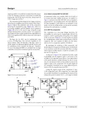
The comparator for this design is a two-stage comparator capacitive DAC, and sampling switch. For each subcircuit,
including a preamplifier stage and the dynamic latch stage. we then developed a test based on the analyzed crucial
19
Figure 6 depicts the schematic view of the comparator, nodes. For the rest of this section, we discuss the test mode
including the preamplifier stage (Figure 6A), which is a developed for each subcircuit in detail.
5-transistor amplifier, and the dynamic latch comparator
(Figure 6B), which is the second stage. Using the design 2.3.3. BIST for comparator
method introduced in a previous paper, the comparator The comparator is a two-stage design, including the
19
was designed to have output resolution for input difference preamplifier for achieving the required gain, followed by
of half least significant bit (LSB) at a maximum clock speed a dynamic latch to speed up the settling time of the output
of 10 MHz. of the comparator (Figure 6). Considering the six defects
The logic for the ADC can be implemented using for complementary metal-oxide-semiconductor (CMOS)
a series of D-flip flops, thus realized completely in the transistors, the total number of defects in the defect
digital domain. Since the domain of the logic control is universe for the comparator equals to 102 defects.
purely digital and advanced digital methods can be used By analyzing the operation of the comparator and
for performing defect detection for this part. Therefore,
for any of the proposed BIST, it is assumed that the logic monitoring the voltages at its different nodes, we developed
control has already been tested and operates as expected. a test operation mode that promises full defect coverage
which requires neither injector circuits for excitation, nor
any monitoring circuits.
As depicted in Figure 6, the comparator’s positive input
is grounded, and the negative input is connected to the
top plate of the capacitive array. Hence, if we want to have
a test mode operation without altering the circuit in any
way, the only nodes to which we have relative access are the
negative input of the comparator (IN_N) and outputs of
the comparator. Moreover, we can assign different specific
values to IN_N, using the capacitive DAC.
Setting the negative input of the comparator to take
+LSB voltage level and -LSB voltage level, we notice that
we can detect the defects by monitoring the outputs of the
Figure 5. Bootstrapped sampling switch comparator, positive output (OUT+), and negative output
A B
Figure 6. Structure of the comparator: (A) Pre-amplifier stage and (B) latch stage
Volume 1 Issue 1 (2024) 6 doi: 10.36922/dp.4351