
Page 69 - DP-1-1
P. 69
Design+ Defect-oriented BIST for AMS circuits
resistor that should be realized as a short circuit in a defect- The resistors R , R , R , R , R , R , and R GG” are
DS
GG
SS
GD
DD
GS
free scenario and therefore has a value of 0 Ω in this case. modeled in Verilog-A. Two new terminals named V and
C
Similarly, in a defect-free situation, R nml_open is realized as an V are defined for them. Based on the model defined,
G
open circuit and ideally must be ∞ Ω (modeled using 0A the values of these resistors are evaluated by defining an
current source). R flt_short acts as a shorted circuit in the case equation in the model that includes the value of (V - V ),
G
C
of a short defect and, depending on the defect model, can the id of the transistor (referred to as fet_id) and the
take a value in the range of 1 Ω to 100 Ω. R flt_open emulates number of defect—0 for defect free to 6—that is required
an open circuit in the case of a defect and, depending on to be tested. With V grounded in the design and allocating
G
the defect model, can have any value greater than 1 MΩ. different fet_id value to each transistor in the circuit under
For instance, when modeling the drain-open defect, the test, we only need to assign an appropriate value for
all the resistors in the model—R , R , R , R , R , and V to emulate a specific defect for a specific transistor in
C
GG
SS
GD
DS
GS
R GG” —take values identical to the defect-free model. R , the design. Using this model, any defect can be tested in
DD
however, takes the value of the open circuit resistor, R flt_open a very short time without changing the configuration of
which is defined as a parametric attribute. the design for testing each defect. The introduced model
also enables consecutive simulations for numerous defect
scenarios, which remarkably reduces the simulation time.
2.3. SAR ADC: A case study
2.3.1. Structure of SAR ADC
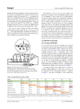
A 12-bit SAR ADC in 65 nm technology was designed
for the demonstration and testing of the proposed digital-
like defect-oriented BIST. Figure 4 depicts the general
structure of the SAR ADC, which includes the binary-
weighted capacitive DAC, a comparator, and a SAR
control. The capacitive DAC is a segmented structure with
two segmented 6-bit binary weighted capacitive segments
for area efficiency. The bottom plate of the capacitive array
in the DAC is either connected to the ground line through
an N-channel Metal-Oxide-Semiconductor (NMOS)
switch, or to the VDD line through a P-channel metal-
oxide-semiconductor (PMOS) or to Vin – sampling signal
– through the sampling switch, as presented in Figure 4.
Figure 4. SAR ADC Structure used as case study The sampling switch used in this work is an enhanced
Abbreviations: ADC: Analog-to-digital converter; Cb: Capacitor constant voltage difference of the gate and source of
bootstrapped; GND: Ground line in the circuit; LSB: Least significant
bit; MSB: Most significant bit; SAR: Successive approximation register; the transistor (VGS) bootstrapped switch, as depicted
Vref: Reference voltage similar to usage of Vin. in Figure 5. The main advantage of this conventional
Table 1. Lookup table for the defect model
Defect R DD R SS R GG R GD R GS R DS R GG
Defect-free R nml_short R nml_short R nml_short R nml_open R nml_open R nml_open R nml_short
Drain-open R R R R R R R
flt_open nml_short nml_short nml_open nml_open nml_open nml_short
Source-open R R R R R R R
nml_short flt_open nml_short nml_open nml_open nml_open nml_short
Gate-open R R ∞ 0.5TΩ 0.5TΩ R 1TΩ
nml_short nml_short nml_open
Gate-drain short R R R R R R R
nml_short nml_short nml_short flt_open nml_open nml_open nml_short
Gate-source short R R R R R R R
nml_short nml_short nml_short nml_open flt_open nml_open nml_short
Drain-source short R nml_short R nml_short R nml_short R nml_open R nml_open R flt_open R nml_short
Note: Green represents value of the resistors for defect-free model, and the other color represents the change of the value of respective resistors for each
defect model from the defect free values, for example, for the drain-open model we only need to change R in the defect free model from R nml_short to
DD
R flt_open , to achieve the drain-open model.
Volume 1 Issue 1 (2024) 5 doi: 10.36922/dp.4351