
Page 74 - DP-1-1
P. 74
Design+ Defect-oriented BIST for AMS circuits
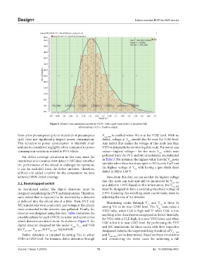
Figure 8. Monte Carlo simulation results for OUT+ with a gate-open defect at transistor M6
Abbreviation: OUT+: Positive output.
from a few picoamperes (pA) to hundreds of picoamperes V out_INV is enabled when Vin is at the VDD level. With no
(pA) does not significantly impact power consumption. defect, voltage at V should also be near the VDD level.
out
This variation in power consumption is relatively small Any defect that makes the voltage of this node less than
and can be considered negligible when compared to power VDD is detectable by monitoring this node. The worst-case
consumption variations related to PVT effects. values—highest voltage— for the node V , which were
out
For defect coverage calculation in this case, since the gathered from the PVT and MC simulations, are indicated
mentioned drain-source short defect in M7 does not affect in Table 3. For instance, the highest value that the V node
out
the performance of the circuit or endanger its operation, can take when there is a drain open in M1 is only 1 µV and
it can be excluded from the defect universe. Therefore, the highest voltage at V with having a gate-drain short
out
without any added circuitry for the comparator, we have defect in M6 is 1.48 V.
achieved 100% defect coverage. Now, from this data, we can see that the highest voltage
that this node can take and still be monitored by V
3.2. Bootstrapped switch as a defect is 1.94V. Based on this information, the V out_INV
out_INV
As mentioned earlier, the digital detectors must be must be designed to have a switching threshold voltage of
designed considering the PVT and mismatches. Therefore, 1.95V. Ensuring this switching point can be easily done by
each defect that is expected to be detected by a detector adjusting the size of the inverter.
is induced into the circuit one at a time. Then, PVT and Monitoring nodes through V and V is done by
MC simulations were conducted, and voltage at the crucial setting Vin to be near GND level. The V node takes a
G1
G8
node connected to the detector was gathered. Finally, the VDD value when CLK is high and ‘0’ when CLK is low,
G1
detector was designed using this data. Table 3 tabulates the anything other than these is categorized as defect. Similarly,
possible defects for each CMOS transistor and summarizes for VG8, with a CLK high, it is near VDD level, and when
which detector can detect them. As shown in Figure 5, the CLK is low it is near GND level. By performing the PVT
digital detector designed for the nodes V , V and VG8 and MC simulations for these nodes with their respective
G1,
out
are V out_INV , V G1_INV and V G8_INV ,respectively. designated defects, the target switching threshold of V
G1_INV
Defect detection is initiated by setting Vin to either and V G8_INV can be determined. Based on these simulations
VDD or GND level. For instance, defect detection through and considering the worst cases for achieving a full
Volume 1 Issue 1 (2024) 10 doi: 10.36922/dp.4351