
Page 73 - DP-1-1
P. 73
Design+ Defect-oriented BIST for AMS circuits
occurrence or different probabilities does not affect the with a -LSB voltage at IN_N, we expect a logic high, or near
defect coverage, as all defects are detected. VDD value, at OUT+. However, in the Figure 8, we can
observe that the voltage at OUT+ for all the 200 cases is less
3.1. Comparator than 2 µV at OUT+, detecting the defect for all the cases.
Table 2 lists the expected outputs of the comparator with From the simulation results, it is clear that all defects
different induced voltage levels given to the IN_N of in the transistors of the pre-amplifier and the dynamic
the comparator. Before conducting any defect coverage latch can be detected, except for the drain-source short
simulation, we ensured that the values of the output remain defect in M7, open-source in M14, and open-gate defect
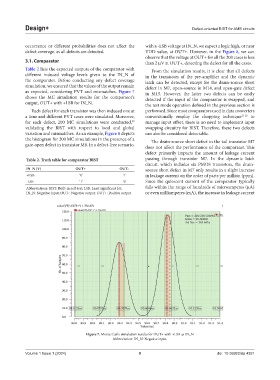
as expected, considering PVT and mismatches. Figure 7 in M15. However, the latter two defects can be easily
shows the MC simulation results for the comparator’s detected if the input of the comparator is swapped, and
output, OUT+ with +LSB for IN_N. the test mode operation defined in the previous section is
Each defect for each transistor was then induced one at performed. Since most comparators used in data converters
a time and different PVT cases were simulated. Moreover, conventionally employ the chopping technique 23-25 to
for each defect, 200 MC simulations were conducted, manage input offset, there is no need to implement input
22
validating the BIST with respect to local and global swapping circuitry for BIST. Therefore, these two defects
variation and mismatches. As an example, Figure 8 depicts can also be considered detectable.
the histogram for 200 MC simulations in the presence of a The drain-source short defect in the tail transistor M7
gate-open defect in transistor M6. In a defect-free scenario, does not affect the performance of the comparator. This
defect primarily impacts the amount of leakage current
Table 2. Truth table for comparator BIST passing through transistor M7. In the dynamic latch
circuit, which includes six PMOS transistors, the drain-
IN_N (V) OUT+ OUT‑ source short defect in M7 only results in a slight increase
+LSB ‘0’ ‘1’ in leakage current on the order of parts per million (ppm).
-LSB ‘1’ ‘0’ Since the quiescent current of the comparator typically
Abbreviations: BIST: Built-in self-test; LSB: Least significant bit; falls within the range of hundreds of microamperes (µA)
IN_N: Negative input; OUT-: Negative output; OUT+: Positive output. or even milliamperes (mA), the increase in leakage current
Figure 7. Monte Carlo simulation results for OUT+ with +LSB as IN_N
Abbreviation: IN_N: Negative input.
Volume 1 Issue 1 (2024) 9 doi: 10.36922/dp.4351