
Page 67 - DP-1-1
P. 67
Design+ Defect-oriented BIST for AMS circuits
operation. The main requirements in designing of BIST
are its transparency with respect to the main circuit. BIST
should have zero effect on the normal operation of the
circuit. In addition to this, BIST should be fast and have
a small area and power overhead in comparison to the
main circuit. For digital circuits, meeting these main BIST
requirements is generally easier compared to AMS circuits,
primarily due to the significantly higher sensitivity of
AMS circuits. Moreover, the occurrence of a defect has
a more noticeable effect on a digital circuit. Most of the
hard defects in digital circuits would be manifested by a
stuck-on high or stuck-on low logic, which can be detected
with near zero additional resources. However, in AMS
circuits, a similar defect might not significantly change the
performance of the circuit.
We propose a defect-oriented BIST for AMS circuits that
exclusively utilizes digital circuits, resulting in lower power
consumption and typically smaller area requirements
compared to AMS circuits. In addition, digital-like AMS
BIST can itself be tested using digital methods before
performing the test on the AMS circuits. Furthermore,
the digital-like AMS BIST is also easier to migrate from
one technology node to another, reducing the need for a
redesign of BIST. Using digital-like BIST, the result of the
test can be easily routed for inference within IC using well-
defined digital protocols.
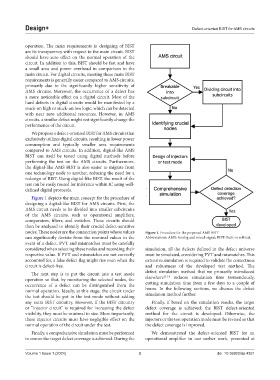
Figure 1 depicts the main concept for the procedure of
designing a digital-like BIST for AMS circuits. First, the
AMS circuit needs to be divided into smaller subcircuits
of the AMS circuits, such as operational amplifiers,
comparators, filters, and switches. These circuits should
then be analyzed to identify their crucial defect-sensitive
nodes. These nodes are the connection points whose values Figure 1. Procedure for the proposed AMS BIST
can significantly deviate from the nominal values in the Abbreviations: AMS: Analog and mixed-signal; BIST: Built-in self-test.
event of a defect. PVT and mismatches must be carefully
considered when selecting these nodes and recording their simulation, all the defects defined in the defect universe
respective value. If PVT and mismatches are not correctly must be simulated, considering PVT and mismatches. This
accounted for, a false defect flag might rise even when the extensive simulation is required to validate the correctness
circuit is defect-free. and robustness of the developed test method. The
The next step is to put the circuit into a test mode defect simulation method that we primarily introduced
operation so that, by monitoring the selected nodes, the elsewhere 12-14 reduces simulation time tremendously,
occurrence of a defect can be distinguished from the cutting simulation time from a few days to a couple of
normal operation. Ideally, at this stage, the circuit under hours. In the following sections, we discuss the defect
the test should be put in the test mode without adding simulation method further.
any extra BIST circuitry. However, if the BIST circuitry Finally, if based on the simulation results, the target
or “injector circuit” is required for increasing the defect defect coverage is achieved; the BIST defect-oriented
visibility, they must be minimal in size. More importantly, method for the circuit is developed. Otherwise, the
these injector circuits must have negligible effect on the injectors or the test operation mode must be revised so that
normal operation of the circuit under the test. the defect coverage is improved.
Finally, a comprehensive simulation must be performed We demonstrated the defect-oriented BIST for an
to ensure the target defect coverage is achieved. During the operational amplifier in our earlier work, presented at
Volume 1 Issue 1 (2024) 3 doi: 10.36922/dp.4351