
Page 66 - MSAM-4-1
P. 66
Materials Science in Additive Manufacturing In situ electromagnetic field manipulation during LMD
600 #, 1200 #, and 4000 # sandpaper in turn) and polished were tested for each sample (Figure 2E). The distance
using OPS (SiO suspension) with 40% H O as volume between each test point was 0.4 mm, and the selected
2
2
2
fraction. Before the microstructure characterization, position of the highest point was 0.4 mm from the top of
the sample was immersed in an etchant solution the deposition layer.
(V :HNO :H O=3:5:92) for 60 – 70 s. The microstructure
2
3
HF
characterization was conducted using a scanning electron 3. Results and discussion
microscope (JSM-IT800, HL; Japan). The upper (U), middle 3.1. Morphological analysis of the molten pool
(M), and bottom (B) areas of the deposition layer were
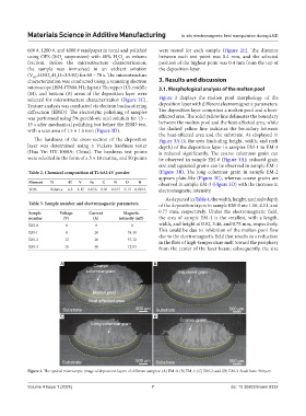
selected for microstructure characterization (Figure 2C). Figure 3 displays the molten pool morphology of the
Texture analysis was conducted via electron backscattering deposition layer with different electromagnetic parameters.
diffraction (EBSD). The electrolytic polishing of samples The deposition layer comprises a molten pool and a heat-
was performed using 5% perchloric acid solution for 13 – affected area. The solid yellow line delineates the boundary
15 s after mechanical polishing but before the EBSD test, between the molten pool and the heat-affected area, while
with a scan area of 1.5 × 1.5 mm (Figure 2D). the dashed yellow line indicates the boundary between
the heat-affected area and the substrate. As displayed in
The hardness of the cross-section of the deposition Figure 3A-D, the area (including height, width, and melt
layer was determined using a Vickers hardness tester depth) of the deposition layer in samples EM-1 to EM-3
(Hua Yin HV-1000A; China). The hardness test points is reduced significantly. The coarse columnar grain can
were selected in the form of a 5 × 10 matrix, and 50 points be observed in sample EM-0 (Figure 3A); reduced grain
size and equiaxed grains can be observed in sample EM-1
Table 2. Chemical composition of Ti-6Al-4V powder (Figure 3B). The long columnar grain in sample EM-2
appears plate-like (Figure 3C), whereas coarse grains are
Element Ti Al V Fe C N O H observed in sample EM-3 (Figure 3D) with the increase in
Wt% Balance 6.2 4.15 0.056 0.01 0.015 0.15 0.0016 electromagnetic intensity.
As depicted in Table 4, the width, height, and melt depth
Table 3. Sample number and electromagnetic parameters of the deposition layers in sample EM-0 are 1.16, 4.11, and
Sample Voltage Current Magnetic 0.77 mm, respectively. Under the electromagnetic field,
number (V) (A) intensity (mT) the area of sample EM-1 is the smallest, with a length,
EM-0 0 0 0 width, and height of 0.92, 3.46, and 0.75 mm, respectively.
EM-1 8 20 39.40 This could be due to inhibition of the molten pool flow
due to the electromagnetic field that results in a reduction
EM-2 12 30 57.12 in the flow of high-temperature melt toward the periphery
EM-3 16 40 72.93 from the center of the laser beam; subsequently, the size
A B
C D
Figure 3. The optical microscopic image of deposition layers of different samples: (A) EM-0; (B) EM-1; (C) EM-2; and (D) EM-3. Scale bars: 500 µm
Volume 4 Issue 1 (2025) 7 doi: 10.36922/msam.8332