
Page 64 - ESAM-1-4
P. 64
Engineering Science in
Additive Manufacturing EST manipulates structure of Ti-6Al-4V/Cu
A D
C
B
E F
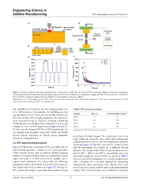
Figure 1. Schematic diagram of the experimental process. (A) Schematic of LMD; (B) schematic of EST; (C) schematic diagram of specimen preparation;
(D) schematic of the microstructural characterization region; (E) EST pulse waveforms; (F) temperature changes after EST in Ti-6Al-4V/Cu-Cr-Zr (EST-0,
EST-1, and EST-2 represent samples treated at different current densities, as shown in Table 2).
Abbreviations: AC: Alternating current; EBSD: Electron backscatter diffraction; EST: Electroshock treatment; LMD: Laser melting deposition; SEM:
Scanning electron microscopy; XRD: X-ray diffraction.
was controlled at 6.9 g/min, and the scanning speed was Table 2. EST parameter settings
set to 300 mm/min. Concurrently, the shielding gas flow 2
was maintained at 25 L/min, and the powder delivery gas Samples Time (s) Current density (A/mm )
flow was 5 L/min. After sample preparation, the specimens EST-0 0 0
were machined using an electrical discharge machining EST-1 0.1 205
(EDM) device into cylinders with a diameter of 5 mm and EST-2 0.1 262
a height of 7 mm for EST experiments (Figure 1B and C). EST-3 0.1 306
To minimize the impact of EDM on EST experiments, the Abbreviation: EST: Electroshock treatment.
cut samples were polished using 600#, 1200#, and 4000#
silicon carbide sandpaper to remove traces generated an infrared thermal imager. The temperature rose to its
during the cutting process. peak within an extremely short time and subsequently
2.2. EST experimental procedure cooled naturally in the air, with the temperature variation
shown in Figure 1F. The EST time was 0.1 s with 5 pulses,
Figure 1D illustrates a schematic of EST assembly, and the and the experiment was carried out at different current
experimental apparatus includes an AC pulse generator, densities. The samples with different current densities were
a Hall current sensor, and an infrared thermal imaging named EST-1, EST-2, and EST-3, respectively, while the
camera. From top to bottom, there are a removable copper untreated sample was named EST-0, as shown in Table 2.
upper electrode, a Ti-6Al-4V/Cu-Cr-Zr sample, and a For each set of EST parameters, five cylindrical specimens
copper lower electrode. AC pulses with the following with a diameter of 5 mm were selected for machining.
parameters can be output: Peak current and pulse frequency. Subsequently, three specimens were chosen from each
The output waveform is shown in Figure 1E. During the set for microstructural analysis and mechanical property
EST process, the sample temperature was monitored using testing. Both microstructure and mechanical properties
Volume 1 Issue 4 (2025) 3 doi: 10.36922/ESAM025430030