
Page 27 - MSAM-3-3
P. 27
Materials Science in Additive Manufacturing Defects in additively fabricated Al6061
A B C
D E F
G H I
J K L
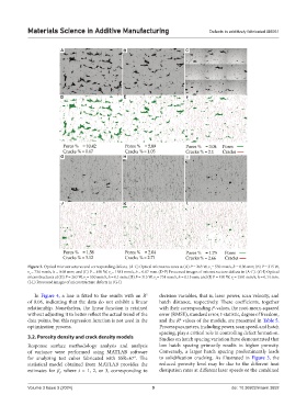
Figure 3. Optical microstructures and corresponding defects. (A-C) Optical microstructures at (A) P = 263 W, v = 550 mm/s, h = 0.06 mm; (B) P = 315 W,
s
v = 734 mm/s, h = 0.08 mm; and (C) P = 490 W, v = 1581 mm/s, h = 0.07 mm. (D-F) Processed images of microstructure defects in (A-C). (G-I) Optical
s
s
microstructures at (G) P = 263 W, v = 550 mm/s, h = 0.1 mm; (H) P = 315 W, v = 734 mm/s, h = 0.15 mm; and (I) P = 490 W, v = 1581 mm/s, h = 0.14 mm.
s
s
s
(J-L) Processed images of microstructure defects in (G-I)
In Figure 4, a line is fitted to the results with an R decision variables, that is, laser power, scan velocity, and
2
of 0.06, indicating that the data do not exhibit a linear hatch distance, respectively. These coefficients, together
relationship. Nonetheless, the linear function is retained with their corresponding P-values, the root-mean-squared
without adjusting it to better reflect the actual trend of the error (RMSE), standard error, t-statistic, degree of freedom,
data points, but this regression function is not used in the and the R values of the models, are presented in Table 5.
2
optimization process. Process parameters, including power, scan speed, and hatch
spacing, play a critical role in controlling defect formation.
3.2. Porosity density and crack density models Studies on hatch spacing variation have demonstrated that
Response surface methodology analysis and analysis low hatch spacing primarily results in higher porosity.
of variance were performed using MATLAB software Conversely, a larger hatch spacing predominantly leads
for analyzing test cubes fabricated with SSR=67°. The to solidification cracking. As illustrated in Figure 3, the
statistical model obtained from MATLAB provides the reduced porosity level may be due to the different heat
estimates for β , where i = 1, 2, or 3, corresponding to dissipation rates at different laser speeds or the combined
i
Volume 3 Issue 3 (2024) 9 doi: 10.36922/msam.3652