
Page 61 - MSAM-3-3
P. 61
Materials Science in Additive Manufacturing In-situ alloying of Ti41Nb by LPBF
scan track across the columns and varying laser scan Machining machine (Troop, Singapore). After visual
speed across the rows. inspection, the set of samples with a hatch spacing of
60 μm was selected for analysis as they presented no visible
2.3. Fabrication of tensile coupon blocks surface warping in the as-built condition. One-half of each
Based on the experimental results from the tile specimens, sample tile was cut from the LPBF base plate, as shown
another set of specimens (tensile coupon blocks) was in Figure 3A, to be used for microstructural analysis. The
fabricated with different process parameters to be machined extracted half-tile samples are shown in Figure 3B.
into tensile specimens. In Table 2, the sample dimensions,
scanning speeds, and scanning pattern for the tensile coupon 2.5. Sample analysis
blocks are shown. The parameter set was designed based on The half-tile specimens were hot-mounted, and the cross-
the hatch spacing of 0.06 μm from the tile specimen where section (perpendicular to the build direction) was revealed.
no obvious defects could be seen from the as-printed parts. They were then polished to a mirror finish using a range
Four scanning velocities, ranging from 317 to 650 mm/s, of coarse (P320) to fine-grit (P4000) sandpapers in a
were deployed, with a constant hatch spacing of 0.06 μm, progressive manner, followed by final polishing with oxide
identical to that of the tile specimens. The main parameter polishing suspension. When required, the samples were
of interest here was the stripe width (of 1 and 10 mm) to etched with Kroll’s reagent to reveal the microstructure.
mimic the innermost region versus the outer region of the An Axioskop 2 MAT optical microscope (OM) was
contour scan-built tile specimens, where 1 mm stripe width used to identify underlying defects and unmelted niobium
will have less thermal delay time than the 10 mm stripe particles on the cross-section. Image processing software,
width. Stripe width refers to the maximum scanning vector ImageJ, was employed to digitally enhance the OM-captured
length; once reached, the laser scans adjacent to the current image, allowing for analysis and quantification of surface
vector is at a distance equal to the hatch spacing. All tensile
specimens were cut in a way that is tested in the direction
perpendicular to the build direction.
The SLM 280 HL machine has an argon flow from right
to left for removing sputtering particles. Hence, to minimize
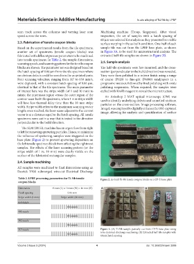
the influence of sputtering, samples were staggered on the
base plate (Figure 2) to prevent sputtering deposition on
the left tensile specimen block from affecting the rightmost
samples. The effects of the laser scanning pattern (or the
stripe width of 1 vs. 10 mm) were clearly visible on the
surface of the fabricated rectangular samples.
2.4. Sample machining
All samples were machined to final dimensions using an
Excetek V850 submerged wire-cut Electrical Discharge
Table 2. LPBF processing parameters for Ti‑Nb tensile Figure 2. As-built Ti-Nb tensile coupon blocks on a CP-Ti base plate
coupon blocks
Dimension 45 mm (L) × 10 mm (W) × 16 mm (H) A B
Hatch spacing 0.06 mm
Stripe width (1 mm) Stripe width (10 mm)
650 mm/s
650 mm/s
481 mm/s
481 mm/s
382 mm/s
382 mm/s
317 mm/s Figure 3. (A) Ti-Nb sample partially cut from CP-Ti base plate using
wire electrical discharge machining. (B) Extracted half-tile samples with
317 mm/s
60 μm hatch spacing
Volume 3 Issue 3 (2024) 4 doi: 10.36922/msam.3506